16-bit A/D converter AD676 that meets the requirements for magnetic field measurement accuracy
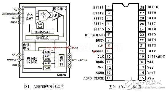
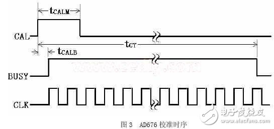
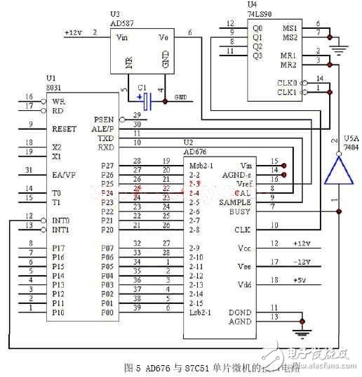
During the measurement of the ship's magnetic field, the intensity of the ship's magnetic field is constantly changing as the ship's motion posture changes. In order to achieve dynamic measurement of the ship's magnetic field, magnetic field measurements must be fast and accurate. The high-speed 16-bit A/D converter AD676, which uses the 87C51 microcontroller to extend the built-in microcontroller, can meet this requirement well. The internal structure of the AD676 is shown in Figure 1. It consists of two monolithic parts, a digitally controlled monolithic and an analog ADC monolithic. The digital control monolith is fabricated using the DXP CMOS process, while the analog ADC monolith is fabricated using the BIMOS II process. The device uses a successive approximation technique to achieve A/D conversion, but there is no traditional resistor ladder network inside, instead it is a capacitor array. The AD676 uses a binary weighted capacitor to distribute the input sampled signal for analog to digital conversion. The use of capacitor arrays brings three benefits: (1). Achieved a high-speed conversion rate of 100KSPS (total conversion time is 10μS); (2). Eliminating the error caused by the resistance value of the traditional resistor network with temperature changes; (3). The capacitor array implements a sample-and-hold function without the need to add external circuitry. However, the capacitor array has an initial error and the internal microprogram controller is designed to eliminate the initial error of the capacitor array. Designed. The microprogram controller detects the matching error of the capacitor array through the DAC, and stores the detected error in the internal data memory RAM. Before the initial data acquisition, the AD676 is automatically calibrated. In the subsequent conversion, the micro The program controller uses the values ​​in RAM to calibrate the resulting digital quantities to improve conversion accuracy. As a result, the AD676 automatically maintains the high performance of the device without user calibration or adjustment. All functions within the AD676, including the actual successive approximation algorithm, auto-calibration, sample-and-hold operation, and output latching of internal data are all under microprogram control. In the application, the user does not need to add additional hardware and software overhead, which brings great convenience to the user. (1). 16-bit no lost code (2). Conversion rate 100KSPS (total conversion time is 10μS) (3). Automatic nonlinear calibration (4). Integral Nonlinearity Error (1NL) ± 1LSB (5). Total harmonic distortion (THD) 0.002% (6). On-chip sampling-and-hold function (7). Full power bandwidth 1MHz. (8). Input analog signal range Vref (9). Power supply range: Vdd = +5V ± 10% Vcc = +12V 5% Vee = -12V 5% The AD676 is available in a 28-pin DIP package and a 28-pin edge brazed ceramic package. The package leads are shown in Figure 2. The AD676 achieves specified performance through on-chip auto-calibration without the need for user calibration and adjustment. The calibration process only needs to be performed once before the initial data acquisition. The calibration timing is shown in Figure 3. When CAL is raised high, the AD676 is internally reset and the BUSY output is high, indicating that the AD676 is ready for calibration. When CAL is applied low, the calibration process begins with a calibration time of 85,530 clock cycles and the calibration is completed with BUSY going low. In most applications, there is sufficient time to calibrate the AD676 only at power-up, so be careful to wait until the power and voltage references are stable before starting calibration. The conversion consists of an input signal acquisition process and a 16-bit internal successive approximation process. Input signal acquisition process: Keep the SAMPLE line high, keep the time ts ≥ 2μS, and then change the SAMPLE line to low level. The input voltage value Vin corresponding to the falling edge of SAMPLE is the actual sample value. After SAMPLE is low, the input Vin is disconnected from the internal capacitor array and the input signal sampling process ends. It is worth noting that during the sampling period, the AD676 ignores the input clock pulse. In the application, to prevent the input clock pulse from interfering with the input signal, it is better to cut off the input of the clock pulse during sampling. 16-bit successive approximation conversion process: Within 17 clock pulses after the SAMPLE line becomes low level tsc time (tsc≥50nS), the AD676 completes the 16-bit successive approximation conversion process, during which the BUSY goes high and the conversion ends. BUSY goes low. When BUSY goes low, the data is output to the BIT1 - BITl6 pin and held until the next conversion begins. Therefore, the result data of this conversion can be read at any time after BUSY goes low until the start of the next conversion. The AD676 has been successfully applied to the ship magnetic field high-speed data acquisition system. Here, the interface circuit of the AD676 and 87C51 single-chip microcomputer in the system is introduced. The interface circuit is shown in Figure 5. In the figure, the signal processing part circuit, the power processing part circuit and the peripheral circuit are omitted, and the purpose of using the AD676 is emphasized. The 87C51 single-chip microcomputer has a 4K byte program memory EPROM. When no external program memory expansion and data memory expansion are required, the four 8-bit parallel ports P0, P1, P2, and P3 of the 87C51 are all used by the user. Therefore, with the interface of 87C51 and AD676, it is possible to design a high-speed and high-precision data acquisition device for ship magnetic field with small size and low power consumption. It is also suitable for applications where volume, power, speed and accuracy are critical. Such as oil well detection, seismic data acquisition, valuable weight measurement and other high-precision measuring instruments. The output of the AD676 does not have a tri-state function, but its output logic is compatible with CMOS and TTL. Therefore, the BIT1-BIT16 of the AD676 can be directly connected to the P0 port and the P2 port of the 87C51. If the AD676 is interfaced with the 8031, the two 8-bit input ports should be extended, and the BIT1-BIT16 of the AD676 should be led to the data bus (P0 port) of the 8031 ​​via the input interface. The calibration control CAL and the conversion control SAMPLE can be connected to either the P1 or P3 port. For example, the calibration CAL is controlled by P3.0, the SAMPLE is controlled by P3.1, and the conversion end signal BUSY is connected to the external interrupt INT0. BUSY also controls the input of the clock pulse signal. As shown in Figure 5, when BUSY is low, the counter 74LS90 will stop working. The AD587 provides a 10V voltage reference. If you use a 5V voltage reference, you can use the AD586 instead of the AD587. From the above analysis, it is not difficult to write the AD676 calibration program and data acquisition conversion program. The calibration procedure is as follows: CLR P3.1; keep SAMPLE low SETB P3.0; preparation for calibration CLR P3.0; start calibration JB P3.2, $; waiting for calibration The data acquisition and conversion process can be written by query mode or interrupt mode. The program segment written by query mode is as follows: SETB P3.1; turn on Vin to charge the capacitor array NOP NOP; wait 2μs CLR P3.1; start conversion JB P3.2, $; waiting for conversion MOV @R0, P2; store high 8-bit data INC R0 MOV @R0, P0; store low 8-bit data ... The AD676 application method designed in this paper can fully utilize its internal functions. If the internal capacitor array is used, the ship's magnetic field can be dynamically measured without an external sample holder, and the built-in microcontroller can be used to verify the linearity before the measurement. High measurement accuracy is achieved with its high resolution. The application of the AD676 simplifies circuit design, reduces manufacturing costs, and effectively improves the performance of the ship's magnetic field measurement system.
High temperature wire is made of high temperature resistance and high strength by special process. It is characterized by high temperature resistance, insulation, fire resistance, flame retardancy, corrosion resistance, aging resistance, weather resistance, high strength, high modulus, anti-static, smooth appearance, etc. High temperature wire generally has two kinds of materials, one is silicone rubber, with good softness; Another is: Teflon (PTFE), which is hard.
Silicone rubber can be used for the installation and connection of electrical circuits with AC rated voltage of 500 V and below, and is widely used in electric heating appliances, paint baking rooms, lighting equipment and household appliances.
Teflon materials can be used in instruments, aerospace, electric power smelting, chemical industry, ships, vehicles, food machinery, household appliances, baking rooms, etc.
Flexible Silicone Wire,Tinned Copper Cable,Silicone Rubber Cable,Flexible Silicone Rubber Wire Ruitian Cable CO.,LTD. , https://www.hbruitiancable.com

