AD630 realizes internal measurement of battery internal resistance
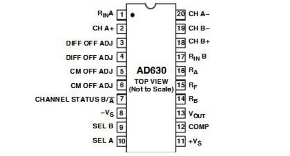
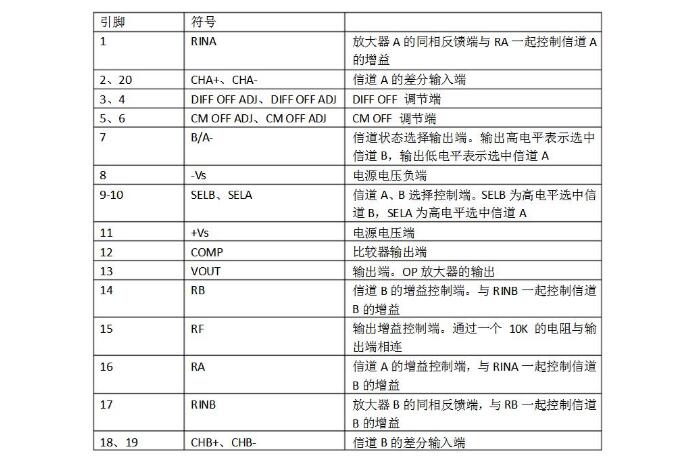
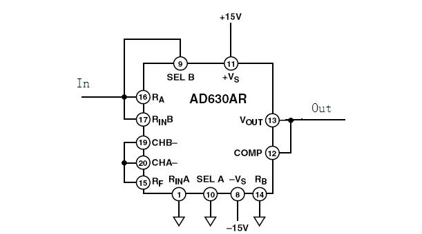
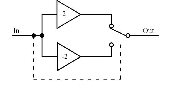
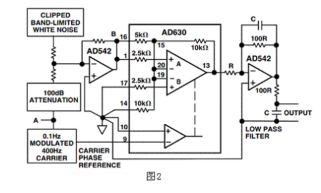
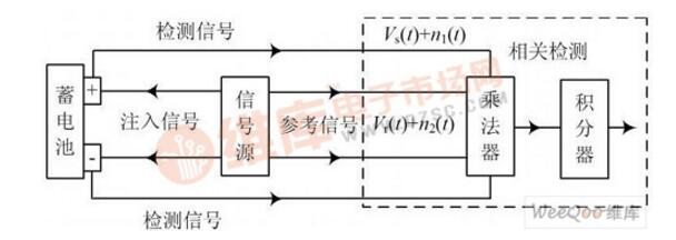
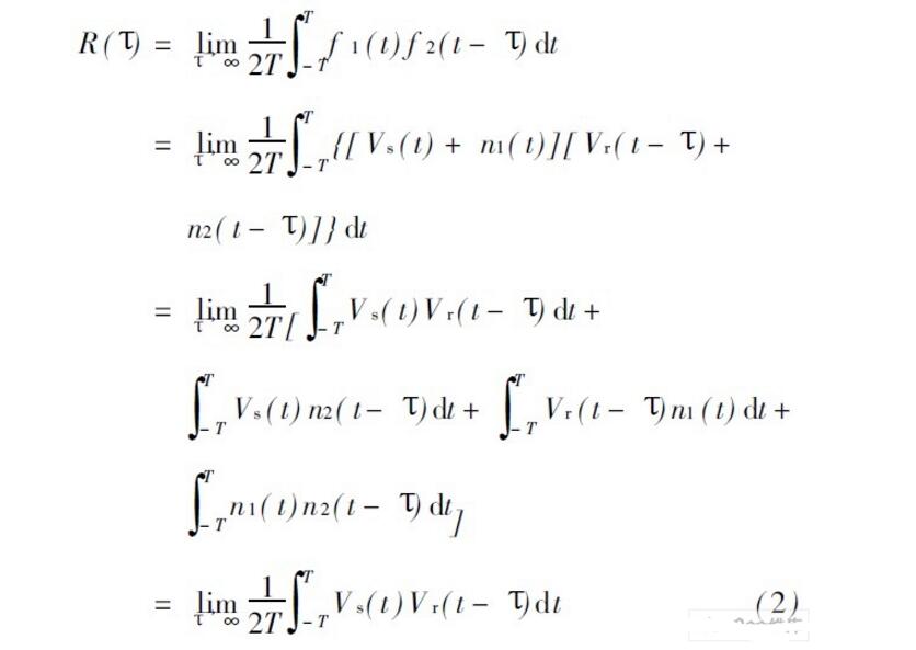
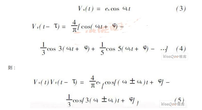
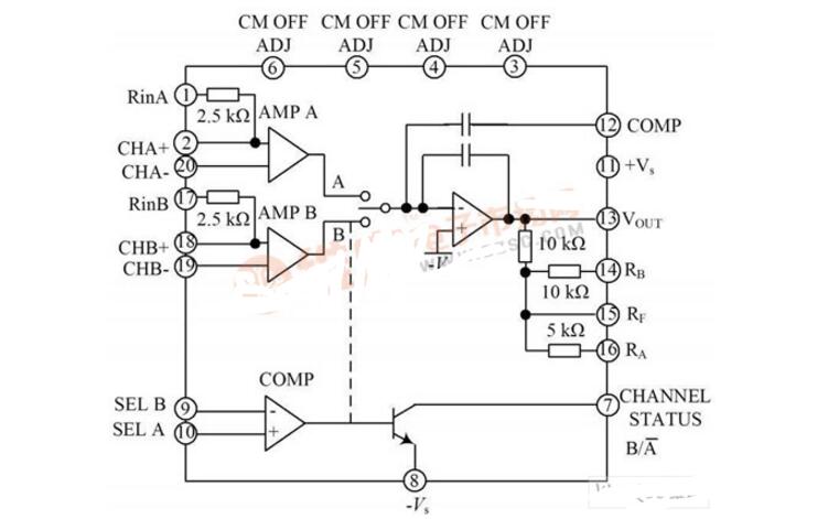
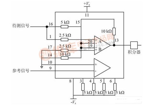
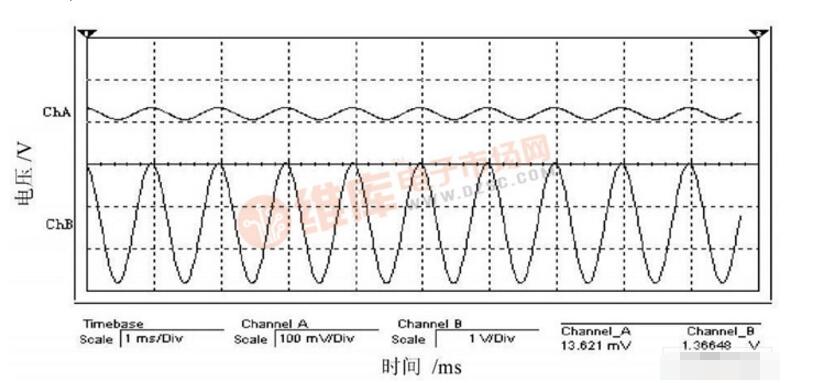
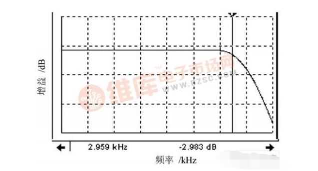
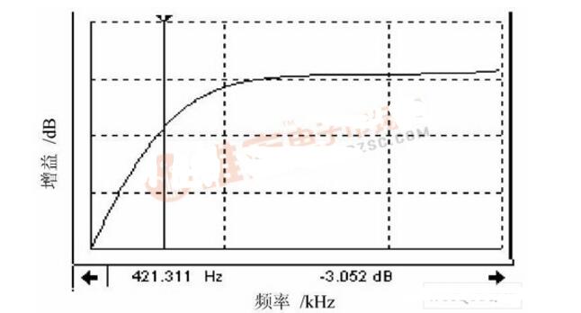
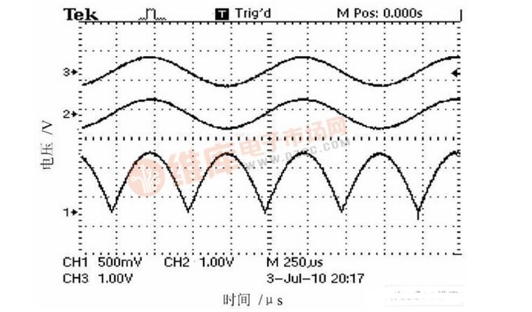
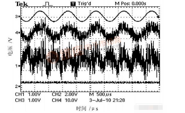
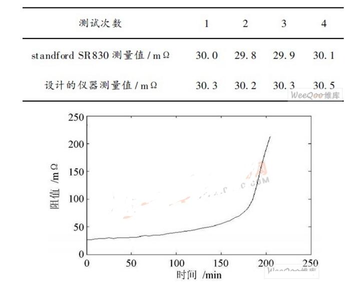
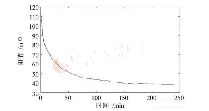
1 can recover the signal from 100dB noise; 2 channel bandwidth: 2Mhz; 3 slew rate: 45V/us; 4 crosstalk: -120dB (1kHz); 5-pin programmable, closed-loop gain: ±1 and ±2; 6 closed-loop gain accuracy and matching: 0.05%; 7-channel offset voltage: 100μV (AD630BD); 8350kHz full power bandwidth. The working principle of this circuit can be illustrated by the following figure. The two op amps inside the AD630 form the same forward and reverse amplifier with a gain of 2, and then use an analog switch to switch between these two. When the input signal is positive, the analog switch hits the end of the non-inverting amplifier. When the input signal is negative, the analog switch hits the end of the inverting amplifier. The above circuit has a gain of 2, and the AD630 can also achieve gains of other multiples. Not much introduced here, there is a need to refer to the AD630 chip manual. This circuit can work in the input signal frequency range from DC to several hundred kHz. The best operating frequency range is from DC to a few kHz. In this band, the effect of this circuit should be the best among these precision rectifying circuits. The input impedance of the above circuit varies with the polarity of the input voltage. When the input voltage is positive, the input impedance is high, and when the input voltage is negative, the input impedance is low. Therefore, there is a certain requirement on the output impedance of the signal source. If the output impedance of the input signal is high, an increase in buffer level is required. AD630 lock-in amplifier circuit schematic shown in Figure 2. The waveform at point A is the bilaterally modulated waveform modulated by the detected signal and the carrier, and the point B is the waveform of the bilateral modulated waveform and the noise superimposed. The pin 9 of the AD630 is connected to the carrier signal, and the square wave and sine wave are all feasible. With a reference phase. The output of the AD630 is connected to an integrating circuit and a low-pass filter to achieve perfect recovery of the signal. The basic principle of implementing online measurement of battery internal resistance is shown in Figure 1. Figure 1 Block diagram of battery internal resistance measurement When the signal source injects an alternating current signal to the battery, the AC voltage signal and the input current generated at both ends of the battery are measured to calculate the internal resistance of the battery: Where: Vrms is the effective value of the AC voltage signal at both ends of the battery; Irms is the effective value of the AC current signal in the input battery. Measuring the internal resistance of the battery using the AC method does not require the battery to be discharged. Theoretically, the battery can be measured in any state. In actual measurement, because the internal resistance of the battery is in micro-Europe or milliohm-class, after injecting a certain current, the voltage signal generated at both ends of the battery is very weak, often being submerged by noise, and then measured after amplification, using an AC voltmeter. Difficult to distinguish between useful signals, you need to use the principle of related detection, in order to measure the AC voltage signal across the battery. The principle of using a correlator to detect weak signals is shown in the relevant detection part of Fig. 1. It is composed of a switch multiplier and an integrator. The weak signal detected at both ends of the battery is input to the multiplier signal input terminal after being pre-amplified and filtered. The sine wave signal injected into the battery is converted into a square wave signal by the circuit and then input to the multiplier reference signal. If the useful signal at both ends of the battery is Vs(t) and the mixed noise is n1(t), the mixed signal at the input is f1(t)=Vs(t)+n1(t); the useful signal at the reference is Vr(t). -τ); When the mixed noise is n2(t-τ), the mixed signal at the reference is f2(t-τ)=Vr(t-τ)+n2(t-τ). According to the principle of correlation detection, multiplication by a multiplier, the signal and noise, noise and noise are mutually independent, their correlation function is zero, only the signal and the signal are related, and can be detected from the noise. Specifically can be expressed as: When the sinusoidal signal detected at both ends of the battery is Vs(t), the square wave reference signal is Vr(t-τ): Because the signal frequency at both ends of the battery is the same as the fundamental frequency of the reference signal, ie ωr=ωs, the output of the integrator is: Where: K is only related to the transmission coefficient of the integrator; φ is the phase difference between the detection signal and the reference signal. If φ=0 is adjusted, the output DC signal reaches its maximum value, which fully shows that after the multiplier and integrator are passed, the noise is suppressed. When the input signal and the circuit transmission coefficient are fixed, the output signal is only proportional to the internal resistance of the battery. As long as the AC voltage across the battery and the AC current through the battery are measured, the internal resistance of the battery can be calculated. To achieve online measurement. A system block diagram designed based on the above principle is shown in FIG. 2 , and includes a path selection switch circuit, a preamplifier band-pass filter, an AD630 multiplier circuit, an integrator circuit, an AC constant current signal generation circuit, and a square wave conversion circuit. Sampling circuit, SCM control system and external display communication and other components. Since the internal resistance of the battery is very small, the influence of the impedance of the wire on the internal resistance of the battery must be reduced, so a four-lead connection method is used. The AC constant current signal output from the system is connected to both ends of the battery, and the voltage signal generated by the battery internal resistance is connected to the input conversion switch circuit. After power-on, the phase difference between the detection signal and the reference signal is first adjusted by the single-chip microcomputer! Make it 0. After the measurement is started, the current measurement path is first strobed by the analog switch CD4052. This path sets a standard sampling resistance in the circuit that injects alternating current signals into the battery to measure the current value of the alternating current signal; then, the voltage measurement path is selected and the voltage value is measured. . The collected signal is sent to the SCM after amplification and filtering, and the internal resistance of the battery is calculated using equation (1). Figure 2 Battery Block Resistance Online Measurement System Block Diagram 2.1 amplification filter circuit Because the collected signal is very weak, it must first carry out the pre-amplification filtering and then enter the correlator. As shown in Figure 3, the low-noise preamplifier consists of an instrumentation amplifier AD620 and a bandpass filter. Figure 3 front signal amplifier circuit schematic The AD620 is a high-performance instrumentation amplifier with stable performance and adjustable gain. The amplification factor is determined by the resistance RG between pin 1 and pin 8. G=1+(49.4kΩ/RG). After the signal is amplified, a band-pass signal of 0.4~3 kHz is detected by the band-pass filter and sent to the signal end of the multiplier. The DC amplifier circuit uses a high-precision op amp OP27 to achieve programmable gain amplification. The feedback resistor of the amplifier is selected using the analog switch CD4052, and the amplification factor is selected by the MCU so that the signal is within the optimal A/D acquisition voltage range. 2.2 correlation operation circuit In the design, the correlator adopts AD630 produced by AD Company, which is a high-precision balanced modulator. The internal resistance is a high-stability SiCr thin film resistor, which ensures the accuracy and stability of its work. Its signal processing applications include balanced modulation and demodulation, synchronous detection, phase detection, quadrature detection, phase sensitive detection, lock amplification, and square wave multiplication. The AD630 logic diagram is shown in Figure 4. It can be thought of as an internal integration of two preamplifiers, a precision comparator for gating preamplifiers, and a multiplexer and output stage integrating op amp. With a high switching speed and a fast and stable linear amplifier, switching distortion can be minimized due to the fast response time of the comparator. In addition, there is extremely low channel-to-channel crosstalk. The AD630 is typically used for high-precision signal processing and wide dynamic range instrumentation. In the lock-in amplifier circuit, when it is used as a synchronous demodulator, weak signals in a noise background of 100dB can be recovered. The optimal operating frequency of the AD630 is at 1 kHz. Therefore, the signal injected into the battery and the reference signal are selected to be 1 kHz. At the same time, 1 kHz is also in the proper frequency response range of the internal resistance of the battery, but it can still work normally at a few tens of megahertz. Using AD630 as a multiplier to achieve the relevant detection circuit schematic shown in Figure 5. Among them, AMPA and AMPB are configured as positive phase amplifier and inverting amplifier respectively. The input signal is a signal to be detected and a reference signal. The signal to be detected is fed through pin 1 and the reference signal is input to the comparator amplifier via pin 9. The signal to be detected is inverted within the device based on the positive and negative carrier signal to achieve a switching multiplication function. Figure 4 AD630 device logic diagram Figure 5AD630 implementation related detection circuit schematic 3.1 Pre-amplification and filtering results analysis The pre-amplification requirement in the design is 100 times. According to the RG calculation formula of RG=49.4kΩ/(G-1) in AD620, RG is 499Ω. Here, the amplifier circuit with a capacitance error of #5% and a resistance error of ±1% is simulated with MulTIsim software. As shown in FIG. 6, channel A is an input signal, and channel B is an output signal amplified by the AD620, if input The effective signal value is 13.621mV, and the output is 1.36*8V, which can achieve accurate and stable amplification. Figure 6 AD620 achieve accurate and stable amplification waveform 3.2 Bandpass Filtering Results Analysis Band-pass filtering is implemented by a first-order low-pass filter and a first-order high-pass filter. The low-pass filter uses a multiple feedback LPF, as shown in U3 of Figure 3, and it can be solved that the filter transfer function is: Let R1 = R2 = R3 = R, C1 = C2 = C, available: Since the passband was cut off at the time, the cutoff frequency was solvable at f=037/(2RC). According to the design requirements, select R = 20kΩ, C = 1nF, the frequency characteristics of the simulation obtained as shown in Figure 7. Figure 7 Low-pass filter frequency characteristics It can be seen from Fig. 7 that when the gain is -3 dB, the corresponding frequency is 3 kHz, and the homogenously designed high-pass filter frequency characteristic is shown in Fig.8. Figure 8 High-pass filter frequency characteristics 3.3AD630 results analysis According to AD630 design requirements to connect a good circuit to achieve the multiplication effect shown in Figure 9, channel 3 is the input signal, channel 2 is the reference signal, channel 1 is the output signal, the signal terminal and the reference input 1 kHz sine signal, the output is two The result of signal multiplication. After multiplication by the AD630, the multiplied signal is sent to the integrator, which filters out the noise and converts it into a DC signal. 30dB noise is mixed in the signal, and the correlator detected by using the AD630 as the core is shown in Fig. 10. Channel 3 is the original signal, channels 4 and 1 are the mixed noise and the signal waveform after passing through the AD630, and channel 2 is the integral. After the DC signal, its value is equal to the value of the original signal passing the correlation detection. This design suppresses noise well and the desired signal can be well detected in the internal resistance measurement system. Figure 9 AD630 multiplier input/output waveform Figure 10 Correlator detection performance 3.4 System Test Results Analysis An on-line measurement system for battery internal resistance was designed and designed according to the scheme in the paper, and compared with the results measured with stanford SR830. The test battery was used for about one year of Universal brand 12V, 15A·h lead-acid batteries. The test results are shown in Table 1. From the measurement data in Table 1, it can be seen that the measurement results of the system and stanford SR830 are basically consistent. Figure 11 is a graph of the internal resistance of a 6V, 4.5A•h battery during on-line measurement. The battery is fully charged and discharged. The discharge current is selected to be 650mA. During the discharge, the internal resistance gradually increases, and the internal resistance change rate is very small at the beginning of the discharge, and it begins to change significantly at the later stage. When the remaining capacity of the battery is more than 50%, the internal resistance value changes very little. When the capacity drops below 40%, the internal resistance value changes significantly. Especially when the battery capacity is less than 20%, the internal resistance value decreases. Sharply increase, at this time should pay attention to charging the battery in time to avoid damage to the battery. Table 1 Comparison of internal resistance test results Figure 11 Discharge characteristics of battery internal resistance Figure 12 is a graph of the internal resistance of the battery during charging. After the battery is discharged to the cutoff voltage, 200mA is selected to charge it, and the internal resistance is measured on-line during the charging process. From the test results, it can be seen that the charge process and the discharge process are exactly the opposite. At the beginning, the internal resistance first decreases drastically, then slowly, and finally almost unchanged. The same change in internal resistance shows the change in capacity. Figure 12 Charging characteristics of internal battery resistance
ZGAR Aurora 1800 Puffs
ZGAR electronic cigarette uses high-tech R&D, food grade disposable pod device and high-quality raw material. All package designs are Original IP. Our designer team is from Hong Kong. We have very high requirements for product quality, flavors taste and packaging design. The E-liquid is imported, materials are food grade, and assembly plant is medical-grade dust-free workshops.
Our products include disposable e-cigarettes, rechargeable e-cigarettes, rechargreable disposable vape pen, and various of flavors of cigarette cartridges. From 600puffs to 5000puffs, ZGAR bar Disposable offer high-tech R&D, E-cigarette improves battery capacity, We offer various of flavors and support customization. And printing designs can be customized. We have our own professional team and competitive quotations for any OEM or ODM works.
We supply OEM rechargeable disposable vape pen,OEM disposable electronic cigarette,ODM disposable vape pen,ODM disposable electronic cigarette,OEM/ODM vape pen e-cigarette,OEM/ODM atomizer device.
Aurora 1800 Puffs,Pod System Vape,Pos Systems Touch Screen,Empty Disposable Vape Pod System,1800Puffs Pod Vape System ZGAR INTERNATIONAL(HK)CO., LIMITED , https://www.sze-cigarette.com