Quickly build an arbitrary waveform FPGA in a short time
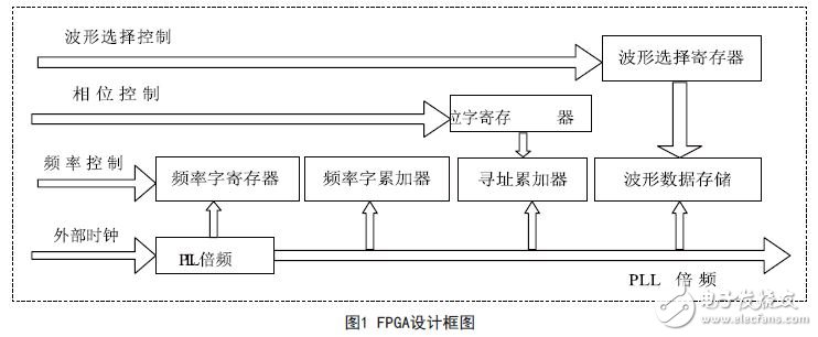
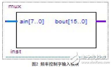
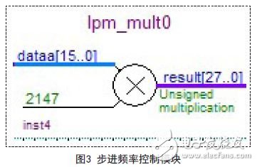
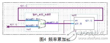
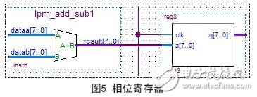
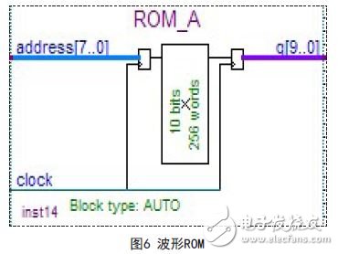
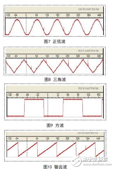
The DDS frequency synthesizer has high frequency resolution and many output frequency points up to 2N frequency points (assuming the word length of the DDS phase accumulator is N); the frequency switching speed is fast, up to us; the phase is continuous when the frequency is switched. The utility model has the advantages that the wide-band orthogonal signal can be output, the output phase noise is low, and the phase noise of the reference frequency source is improved; the arbitrary waveform can be generated; the digitalization is realized, the integration is convenient, the volume is small, and the weight is light. This paper introduces the basic principle of DDS, and briefly introduces the FPGA implementation of DDS waveform generator. The SignalTapII embedded logic analyzer is used to simulate the sine wave, triangle wave, square wave and sawtooth wave. The application of FPGA not only makes the design of digital circuit system very convenient, but also its clock frequency can reach several hundred megahertz. With its flexibility and high reliability, it is very suitable for implementing the digital circuit part of the waveform generator. Using FPGAs to design DDS circuits is more flexible than using dedicated DDS chips. Simply changing the ROM data in the FPGA, DDS can generate arbitrary waveforms with considerable flexibility. The design block diagram of the FPGA is shown in Figure 1. The main function of the FPGA is to generate an interface circuit with the peripheral circuit so that it can accept the peripheral logic control signal; save the frequency word and form a phase accumulator to generate the same frequency as the main clock. RAM addressing word; use internal memory block to form a ROM for storing a plurality of waveform data, and select through a corresponding control line; construct two output channels of multi-waveform selection output, one of which may have a phase shifting function; Use the internal PLL to multiply the external low-frequency crystal oscillator and output the clock at the same frequency as the main clock to drive the off-chip high-speed D/A. According to the Nyquist sampling theorem, a signal with an output frequency of 10 MHz is required, and the input signal clock frequency must be above 20 MHz. The higher the sampling frequency, the better the flatness of the output waveform, and the more samples the waveform has, the better the quality of the waveform obtained. The DDS module in this design is a high-speed module, so there is a high requirement for the system clock, not only need to have a higher frequency, but also have a very high stability, if the clock end of the FPGA is directly added a high The frequency crystal oscillator not only has unstable clock, but also has large power consumption and high cost. In this design, the PLL core of Altera Corporation is directly called, and only a low-frequency crystal oscillator is added to the clock end of the FPGA to achieve the system clock requirement through the internal PLL frequency multiplication of the FPGA. The output clock phase offset is within the allowable range. The frequency control word input module is shown in Figure 2. The data selector controls the input of the 16-bit frequency control word. Step frequency control module shown in Figure 3, through a multiplier to control the step frequency, the specific algorithm is as follows: f step = fc * 2147 / 232. The step frequency is changed by changing the multiplier of the multiplier. To make the stepping to 1 Hz then the multiplier of the multiplier is 22. The frequency accumulator module is shown in Figure 4. The frequency accumulator is formed by a 32-bit adder and a 32-bit register. The frequency control word height is 4 bits. The phase register module is shown in Figure 5. The 8-bit adder and the 8-bit register form the phase register and generate an 8-bit waveform data address. The waveform data ROM is the memory for storing the waveform data. Most of the waveform generator products store the waveform data in the external ROM, so that the structure of each part is clear, the test and maintenance are more convenient, but the shortcoming of the ROM itself is slow. In order to solve the above problems, the whole system uses ROM to design ROM, store waveform data in FPGA, and use the Mega Wizard Plug-In Manager in Quartus II9.0 to generate a ROM. As shown in Figure 6. Mega Wizard Plug-In Manager settings, according to the design requirements, after a seven-step setup, you can generate a ROM IP core. After the amplitude value of one cycle of the desired waveform is solidified in the waveform ROM, the address generated by the address generator addresses the waveform ROM, and can be taken out to D/A conversion and filtered to obtain the desired analog waveform. Output. There are two ways to calculate waveform data: C language and matlab calculation. According to the system design of Section 2, the design program is downloaded to the FPGA chip, and the simulation is performed by using the Quartus II software with SignalTapII embedded logic analysis. The signal waveform is observed. The sine wave is shown in Fig. 7, the triangular wave is shown in Fig. 8, and the square wave is shown in Fig. 9. The sawtooth wave is shown in Figure 10. The experimental results show that the waveform synthesized by DDS technology has good stability, easy to control and adjust. The FPGA can quickly build arbitrary waveforms in a short time, which improves the design efficiency and has practical application value. Board-To-Board Connectors,Machine-Pin Board-To-Board Connectors,Gold Plated Board-To-Board Connectors,8 Pin Board-To-Board Connectors Shenzhen Jinyicheng Electronci Technology Co.,Ltd. , https://www.jycconnector.com