Dry goods! Analysis of Characteristics of Gold Wire Bonded RF Interconnects
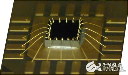
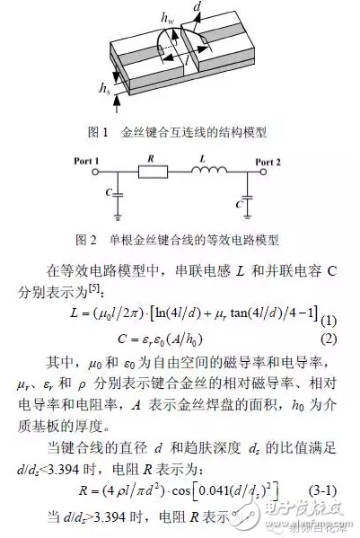
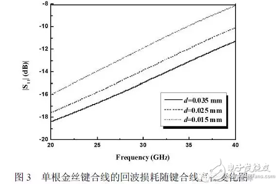
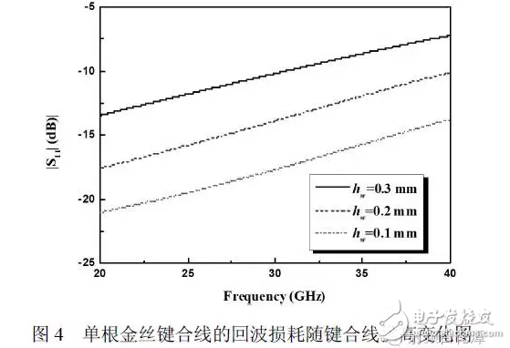
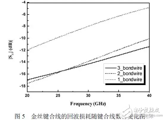
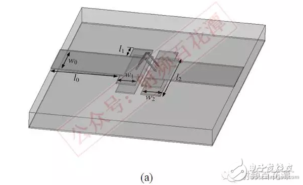
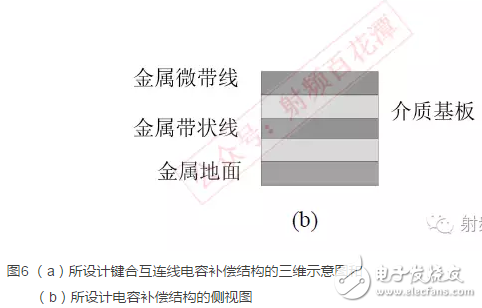
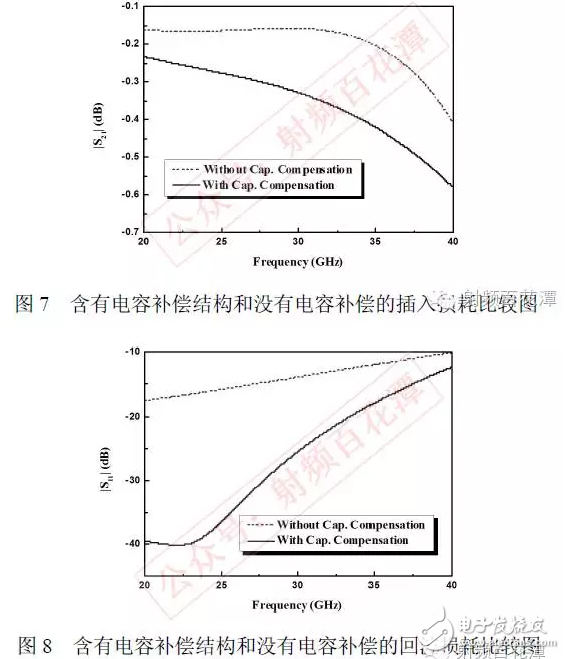
In the fields of radar, electronic countermeasures, and communications, electronic systems are gradually moving toward high density, high speed, high reliability, high performance, and low cost. As a representative of hybrid circuit integration technology, a multi-chip circuit can use a micro-assembly interconnect process to design a bare chip and various components into a microwave integrated circuit that meets requirements in a three-dimensional, multi-layer dielectric substrate. In microwave multi-chip circuit technology, gold wire bonding technology is often used to realize the interconnection between microstrip transmission lines, monolithic microwave integrated circuits and lumped components. Different from the interconnects in the digital circuit, the parameters of the key alloy wire such as the number, length, height of the arch, span, and position of the solder joint have a serious influence on the microwave transmission characteristics. Especially in the high frequency range such as the millimeter wave, the parasitic inductance effect of the key alloy wire is especially obvious. Therefore, analyzing the electromagnetic properties of the gold wire bonding and effectively designing the gold wire interconnection circuit is of great significance for realizing and improving the performance of the multi-chip circuit [1]. There are many methods available for analyzing and improving the electromagnetic properties of key alloy wires in multi-chip circuits. In 1995, Lee used the method of moments to calculate the impedance loss and radiation loss of bond wires, which was used to analyze the broadband electromagnetic characteristics of arbitrary shape interconnects [2]. In the same year, F. AlimenTI et al. proposed the quasi-static method to analyze the transmission characteristics of key alloy wires [3]. Since the dielectric boundary of the bond wire is open and the structure is curved, as the operating frequency increases and the gold wire interconnection parameters change, the accuracy of the above method will also be affected. Subsequently, in 2001, F. AlimenTI et al. proposed to analyze the electromagnetic properties of gold wire bonding using the finite-difference time-domain method [4]. To compensate for the parasitic inductance effect of the bond wire, various methods have been proposed, such as increasing the pad size, increasing the microstrip adjustment branch line, increasing the high and low impedance transmission lines to design the low-pass filter, etc. [5]-[7] . Firstly, this paper uses the method of road to model and analyze the transmission characteristics of the key alloy wire, and then designs the capacitance compensation structure to improve the transmission line and chip, transmission line and transmission line according to the parasitic inductance effect of the gold wire interconnection. Microwave characteristics. Through the calculation results, using this method to design the key alloy wire can effectively improve the transmission performance of the multi-chip circuit. As shown in Figure 1, it is a structural model of a typical gold wire bonding interconnect. A single key alloy wire interconnection is used between two adjacent chips or transmission lines. The length of the gold wire is l, and the diameter is d; the distance between the gold wire and the ground is hs. The corresponding equivalent circuit model is shown in FIG. 2 , in which the key alloy wire can be equivalent to the series resistance R and the series inductance L, and the pads on both sides of the bond wire are equivalent to two parallel capacitors C1 and C2. Since the skin depth is inversely proportional to the square root of the frequency, it can be known from equations (1)-(4) that L and C are less affected by frequency and R is changed with the square root of frequency. In addition, the geometrical parameters of the bond wire will also affect its equivalent inductance, capacitance, and resistance, as well as the interconnection characteristics. As shown in Fig. 3, the effect of the diameter change of a single gold wire bond wire on the return loss of the transmission line. As the diameter d of the key alloy wire increases, the equivalent inductance L decreases, R decreases, the return loss increases, and the insertion loss decreases. Figure 4 shows the effect of the change in the height of a single gold wire bond on the return loss of the transmission line. As the arch height hw of the bond wire increases, the length l of the bond wire increases, L increases, R decreases, the return loss decreases, and the insertion loss increases. As shown in Figure 5, the change in the number of gold wire bonds affects the return loss of the transmission line. With the increase in the number of bond wires, the electromagnetic properties of the interconnections will be significantly improved, but the transmission characteristics above the two gold wires will differ less. According to the above analysis of the characteristics of the gold wire bonding, the diameter of the key alloy wire has a significant effect on the transmission performance; the lower the arch height, the smaller the length of the gold wire and the smaller the transmission loss; and the same, the longer the pitch of the key alloy wire. Small, better interconnection characteristics; insertion loss of multiple gold wires is also apparently due to a single gold wire. From the analysis of the equivalent circuit model of the gold wire bonding interconnection, it can be seen that as the operating frequency increases, especially in the Ka band, the effect of the parasitic inductance of the bonding wire will increase significantly, and the interconnect transmission characteristics will be more Great influence. In order to improve the transmission characteristics of the gold wire, an improved capacitance compensation structure is proposed in this paper. As shown in Figure 6, it is a three-dimensional schematic of the designed compensation structure. Increase the pad size on both sides of the bond wire, and add a corresponding length of metal strip underneath. With this structure, the coupling capacitance can be increased to compensate for the parasitic inductance effect of the bond wire. According to the above method, the capacitive compensation structure of the gold wire bonding interconnection is designed in this paper. The dielectric substrate is a Rogers 5880 material with a dielectric constant of 2.2, a loss tangent of 0.0009, and a substrate thickness of 0.254 mm. The number of gold wire bonds is two, with a diameter of 0.025 mm and a length of 0.3 mm. Full-wave 3D simulation software Ansys HFSS simulation optimization design, finalize the size of the capacitance compensation structure are w1 = 0.3 mm, l1 = 0.3 mm, w2 = 0.3 mm, l2 = 1.32 mm, the width of the 50 ohm microstrip line at the port is w0 = 0.72 mm, l0=1.1 mm. As shown in Figure 7-8, there are two comparison diagrams of the transmission loss and return loss of the two types of capacitors. As can be seen from the figure, in the interconnection structure with 2 bond alloy wires, using the designed capacitance compensation structure, the insertion loss is reduced by approximately 0.1 dB-0.2 dB at the Ka band (20-40 GHz); echo The loss increases by about 23 dB in the frequency range of 20-30 GHz and also increases by 5-10 dB in the higher frequency band. The proposed capacitance compensation structure significantly improves the interconnect transmission characteristics that are degraded due to the parasitic effects of gold wire bonds. This paper presents a capacitance compensation structure for gold wire bonding interconnects. By modeling and analyzing the electromagnetic properties of the bonding interconnects, a capacitive compensation structure is designed to reduce the parasitic inductance effects of the bonding interconnects. Compared with the gold wire without compensation, the designed gold-bonded capacitor compensation structure can significantly improve the transmission characteristics of the wire. In the Ka band, the insertion loss is reduced by 0.1 dB-0.2 dB; the return loss (in the 20-30 GHz frequency range) is increased by about 23 dB. The gold-bonded capacitive compensation structure proposed in this paper can be effectively used in the interconnection design between transmission lines and chips, transmission lines and transmission lines in multi-chip circuits. Liquid Crystal Display For Medical Use Liquid Crystal Display For Medical Use,Super Liquid Crystal Instrument Medical Display,Medical Liquid Crystal Instrument Lcd Display,Thin Transparent Lcd Medical Display Dongguan Yijia Optoelectronics Co., Ltd. , https://www.everbestlcdlcms.com