Method for implementing DDR RAM control and verification using FPGA and IP
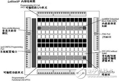
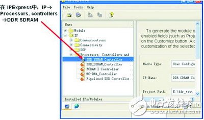
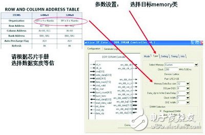
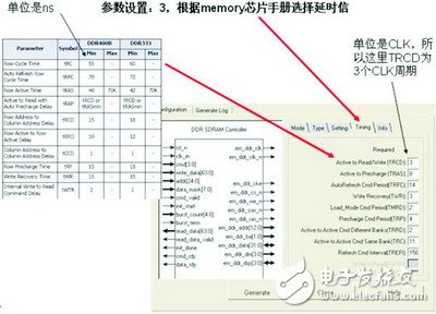
With the continuous development of high-speed processors, the field of embedded system applications is more and more extensive, the scale of digital signal processing is getting larger and larger, and the size of RAM in the system is increasing, such as video surveillance, image data acquisition, etc., image processing. The real-time requirements for RAM bandwidth are increasing. The traditional SDRAM has gradually failed to meet the application requirements in terms of bandwidth. DDR SDRAM (double rate SDRAM) uses the rising and falling edges of the clock CLK signal to perform data transmission on both edges. Traditional SDRAM is only transmitted on the rising edge of the clock, and the transmission bandwidth is doubled. DDR RAM has begun to be widely used in embedded systems and is gradually replacing traditional SDRAM. The increase of DDR RAM operation speed has higher requirements for the design of control timing for designers. Moreover, DDR memory adopts SSTL-II standard supporting 2.5V voltage, and is no longer 3.3V used by SDRAM. Voltage LVTTL standard. There are no DDR RAM controllers on many processors, which makes it harder for designers to use DDR RAM. It is often necessary to insert a controller into the design to implement control of the memory by the microprocessor or DSP. Field Programmable Gate Arrays (FPGAs) have been widely used in embedded systems. Many FPGAs now offer interface features for DDR SDRAM: their input and output pins are compatible with SSTL-II electrical features, and internal hardware resources such as DDR flip-flops and phase-locked loops are provided. Using these features, it is relatively easy to design a reliable high-speed DDR RAM controller. In this paper, we introduce a method to implement DDR RAM control and verification using LatTIce FPGA and IP. LatTIceXP The LatTIceXP device combines a non-volatile FLASH unit with SRAM technology to support instant-on and unlimited reconfigurable single-chip solutions. User profiles are saved in the FLASH cell array. At power-on, the configuration file is transferred from the FLASH memory to the configuration SRAM within 1 millisecond to complete the instantaneous power-up. The device is internally divided into: PIC (programmable I/O unit), nonvolatile FLASH MEMORY, SYSCONFIG configuration port, PFU (programmable function unit), PLL (analog phase-locked loop), PFF (non-RAM/ROM function) Programmable logic unit), EBR (embedded RAM block), JTAG port and other parts (see Figure 1). Figure 1 LatTIceXP internal structure DDR controller IP generation IPExpress is a tool for generating IP modules in Lattice development software. It can generate IP modules based on user-set parameters and is very convenient to use. Click Start IPexpress to enter the build interface (see Figure 2). Select the DDR SDRAM project on the left and set the project name and file save address on the right. Figure 2 IPexpress interface Click Next to begin entering the parameter settings (see Figure 3). This sets the row and column parameters of the DDR RAM, as well as the Bank. These parameters are all set according to the DDR RAM chip manual. The DDR RAM particles used in this paper are Hyundai's HY5DU561622, 16M x16, 4bank pellets. Figure 3 Parameter configuration of row and column of DDR RAM Next, set the timing delay above (see Figure 4). Figure 4 DDR RAM particle timing parameter configuration Set parameters such as tRAC (row access cycle, RAS Access Cycle/Delay), tCAC (column access cycle, CAS Access Cycle/Delay). These parameters are detailed in the manual for the DDR RAM particle chip. It should be specially pointed out that since the chip provider will give different delay parameters for different DDR standards, such as DDR400, DDR333, etc., it will be several different lists in ns, which need to be referenced according to the design. Different forms. Because the IP generator uses a single parameter setting, the unit uses CLK as the unit, which needs to be converted according to the design standard and clock frequency to set. This article uses the DDR266 standard, the clock is 133MHz, the corresponding clock cycle is 1/133MHz, about 7.5ns. Thus, the chip has a TRCD of 20 ns (minimum) in the DDR266 standard, and 3 in the parameters corresponding to the IP. Other parameters are similar conversions.
Anyang Kayo Amorphous Technology Co.,Ltd is located on the ancient city-Anyang. It was founded in 2011 that specializes in producing the magnetic ring of amorphous nanocrystalline and pays attention to scientific research highly,matches manufacture correspondingly and sets the design,development,production and sale in a body.Our major product is the magnetic ring of amorphous nanocrystalline and current transformer which is applied to the communication, home appliances,electric power,automobile and new energy extensively.We are highly praised by our customers for our good quality,high efficiency,excellent scheme,low cost and perfect sale service.
Low Loss Magnetic Ring,Versatile Magnetic Core,High Property Iron Core,High Saturation Iron Core,New Design Iron Core Anyang Kayo Amorphous Technology Co.,Ltd. , https://www.kayoamotech.com


