CMOS RF Model Design Guide
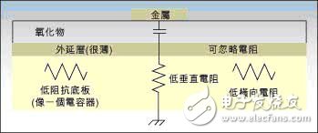
In recent years, we have begun to see some references on radio frequency (RF) CMOS processes and RF model references for these processes. This article will explore the true meaning of this type of RF and explain their importance to RF circuit designers. We can explore RF CMOS design from three perspectives: First, low-frequency analog designers are moving their designs to higher frequencies; second, discrete RF/microwave designers turn to integration; finally, designers will serialize A digital circuit such as a SERDES is raised to the highest frequency that the process can support. In all three cases, RF CMOS design is very helpful, and we will also explain from these perspectives how the RF CMOS itself is different from its modeling. Substrate CMOS applications for traditional digital applications have evolved to use low-resistivity bulk substrates (Figure 1) and to implement a thin, high-resistivity epitaxial layer. This approach often optimizes latch-up (latchup) ) Performance and yield. Figure 1: Basic digital CMOS model built on a low resistivity large substrate as a substrate In order to maintain the flexibility of complex digital circuit routing, multiple metal interconnect layers tend to be uniform in thickness, which allows all metal layers to have nearly identical routing capabilities. This is a relatively ideal substrate for low frequency analog/digital designers: the parasitic capacitance returned from the (grounded) substrate is quite small compared to the capacitive impedance in the band of interest. Therefore, simply extracting parasitic capacitance can very effectively predict actual performance. But RF designers will find four unsatisfactory things: a) the low impedance on the substrate actually maximizes the parasitic capacitance, and the wires formed by the metal interconnects attached to the oxide on the substrate , which ultimately results in a relatively low characteristic impedance; b) the coil built on the substrate is tightly coupled to a shorted coil (ie, the substrate itself), thereby slightly reducing the inductance and Q; c) the current reaching the substrate, Whether it is the capacitive current or the induced current of the coil, it will flow freely over a long distance on a low-resistance substrate; d) efforts to increase the Q value of the coil by paralleling the metal layer have little effect, because if the first use is the most The ideal top layer, then the other additional layers will be closer to the shorted coil of the substrate, so there is almost no substantial improvement in the parallel connection. So, what exactly is the RF CMOS process compared to the general digital variation just described? In many cases, it can simply be thought of as a process that has a high resistivity epitaxial layer throughout the substrate in a typical "digital" process. Now, RF designers have found something completely different: a highly insulated substrate actually creates a second capacitor in series with each parasitic capacitor (since the insulator is thick, so the capacitance is small). It is shunted by a relatively high substrate impedance. The parasitic capacitance acquires a series of additional and important resistance components with some positive effects: large parasitic capacitances such as junction bottom capacitance, which have approximately constant impedance at higher frequencies because the substrate impedance in turn dominates The above capacitive parasitic capacitance; the increase in the Q value of the coil is obviously attributed to the high impedance generated when the substrate short circuit is weakened, and the substrate current tends to be constrained and limited by the significant substrate bypass impedance, thereby improving the insulation. Better results are achieved for parallel metal layers with higher coil Q values. In general, the purpose of increasing the thicker top metal layer (sometimes using higher conductivity copper instead of aluminum) is to significantly increase the coil Q value. Note: Devices constructed with such RF substrates have essentially the same basic characteristics as digital processes. In both cases, the uppermost layers of the device are formed to have the same resistivity. BSIM3 model The BSIM3 model is ubiquitous, and most CMOS designers have been exposed to different versions of the BSIM3 model, such as BSIM3v2 or others. The commercialization of CMOS is very important for its success, because the model organically combines physical and empirical parameters and is easily adaptable to new processes. Physical analysis can predict what happens when the physical scale is reduced, while empirical data allows for a useful approximation of the non-uniform elements of the device being fabricated. Importantly, RF designers need to understand what this important modeling technique means at higher frequencies, so we will next describe how a typical foundry generates such a model. The filling of model parameters is typically accomplished by fabricating devices of various channel widths and lengths and then dc recording the device to generate parameters describing transconductance and impedance. After that, the low frequency capacitance measurement is performed to fill in the capacitive parameters. Typically, model parameters are optimized using an Hspice OpTImizer-optimized optimizer to get the best match between actual data and model data. When the resulting data does not match the expected values ​​within the entire possible scale of the device, the modeler may temporarily bin the model, for example, by making the model at various scales of the device. Branching to form a multi-mode parameter set, each parameter set is optimized over its corresponding smaller device scale range. This makes BSIM3 a "compact model" that adapts well to fast-executing simulators and can be used in layouts with P-cores (physical layout elements with adjustable size parameters) to give designers Great flexibility. PC Battery,Laptop Battery,Tablet Battery,Tablet PC Battery Shenzhen Sunwind Energy Tech Co.,Ltd , https://www.sunwindbatterylm.com